


ATMega328P Microcontroller: A Powerful Microcontroller
 1650
1650
Ⅰ.Introduction
1.1.Overview of ATMega328P
The Atmel® ATmega328P is a low-power CMOS 8-bit microcontroller based on the AVR® enhanced RISC architecture. With the ATmega328P executing powerful instructions in a single clock cycle, the throughput is close to 1MIPS/MHz allowing system designers to optimize power consumption and processing speed.
1.2. Features of ATMega328P
● High-performance, low-power AVR® 8-bit microcontroller
●Advanced RISC architecture
● 131 powerful instructions – most single clock cycle execution
● 32 × 8 general-purpose working registers
● Fully static operation
● Throughput up to 16MIPS at 16MHz
● On-chip 2-cycle multiplier
● High-endurance non-volatile memory segments
● 32K bytes of in-system self-programming flash program memory
● 1Kbytes EEPROM
● 2Kbytes internal SRAM
● Write/erase cycles: 10,000 flash/100,000 EEPROM
● Optional boot code section with independent locking bit
● In-system programming via on-chip bootloader
● True write-and-read operation
● Programming lock ensures software security
●Two 8-bit timers/counters with independent prescalers and compare modes
●16-bit timer/counter with independent prescaler, compare mode and capture function mode
● Real-time counter with independent oscillator
● 6 PWM channels
● 8-channel 10-bit ADC in TQFP and QFN/MLF packages
● Programmable serial USART
● Master/slave SPI serial interface
● Byte-oriented 2-wire serial interface (Phillips I2C compatible)
●Programmable watchdog timer with independent on-chip oscillator
●On-chip analog comparator
● Interrupt and wake-up when pin changes
●Special microcontroller functions
● Power-on reset and programmable undervoltage detection
● Internal calibration oscillator
● External and internal interrupt sources
1.3.ATMega328P Specifications
| core processor | AVR |
| core size | 8-bit |
| speed | 20MHz |
| Connectivity | I²C,SPI,UART/USART |
| peripherals | Undervoltage detection/reset, POR, PWM, WDT |
| Number of I/Os | 23 |
| Program storage capacity | 32KB(16K x 16) |
| Program memory type | flash memory |
| EEPROM capacity | 1K x 8 |
| RAM capacity | 2K x 8 |
| Voltage - Power Supply (Vcc/Vdd) | 1.8 V ~ 5.5 V |
| data converter | A/D 6x10b |
| Oscillator type | internal |
| Operating temperature | -40°C ~ 85°C(TA) |
| Package/casing | 28-DIP (0.300", 7.62mm) |
| Supplier device packaging | 28-PDIP |
1.4.Pin Configurations
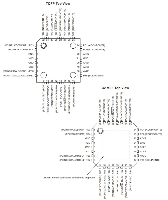
Figure 1-3. Pinout
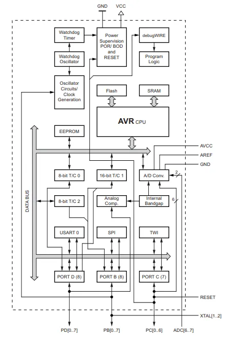
Figure 2-1. Block Diagram
Ⅱ.Architecture of ATMega328P
2.1.Harvard structure of ATMega328P
The ATMega328P uses a Harvard architecture, which means it has two independent memory buses: one for program memory and another for data memory. This structure allows the ATMega328P to access both program and data memory simultaneously, thus improving efficiency. Additionally, because program memory and data memory are separate, data can be read or written without interfering with program execution.
2.2.ATMega328P RISC processor core
ATMega328P uses a modified Harvard structure 8-bit RISC processor core 12. This processor core has the following characteristics:
Simple: The instruction set is streamlined and the instruction execution speed is fast.
Low power consumption: adopts a variety of power-saving technologies, such as sleep mode, etc.
Efficient: able to execute most instructions in one clock cycle.
Programmable: Supports ISP programming method and can be programmed through serial port or parallel port.
Ⅲ.ATMega328P memory
3.1.ATMega328P flash memory
The ATMega328P has 32 KB of ISP flash memory 123. ISP flash memory is an in-system programming (In-System Programming) technology that allows users to program the chip through a serial interface.
3.2.EEPROM of ATMega328P
The ATMega328P has 1 KB EEPROM123. EEPROM is a readable and writable non-volatile memory that retains data after the chip is powered off.
3.3.ATMega328P SRAM
The ATMega328P has 2 KB SRAM123. SRAM is a volatile memory that can lose data when the chip loses power.
Figure 3
Ⅳ.I/O port of ATMega328P
4.1.General purpose I/O lines of ATMega328P
The ATMega328P has 23 general-purpose I/O lines, labeled PB0-PB5, PC0-PC5, and PD0-PD71. These lines can be used as digital input/output lines or for other functions such as PWM output or ADC input.
4.2.General purpose working register of ATMega328P
ATMega328P has 32 general-purpose working registers. These registers are 8-bit and can be used to store data or serve as pointers. The general-purpose working registers are numbered R0-R311.
Ⅴ.Timer/counter of ATMega328P
5.1.Flexible timer/counter for ATMega328P
ATMega328P has 3 flexible timers/counters, namely Timer/Counter 0, Timer/Counter 1 and Timer/Counter 212. Timer/Counter 0 and Timer/Counter 2 are both 8-bit timer/counters with a maximum value of 255 ;And Timer/Counter 1 is a 16-bit timer/counter with a maximum value of 65,53512.
Ⅵ.ATMega328P interrupt system
The ATmega328P supports 25 different interrupt sources. These interrupts and separate reset vectors each have a separate program vector located at the lowest address in the Flash program memory space. A complete list of vectors is shown in Table 11-6, “Reset and Interrupt Vectors in ATMega328P”. Each interrupt vector occupies two instruction words.
This list also determines the priority of different interrupts. The lower the address, the higher the priority. RESET has the highest priority, followed by INT0 – external interrupt request 0.
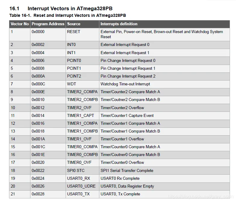
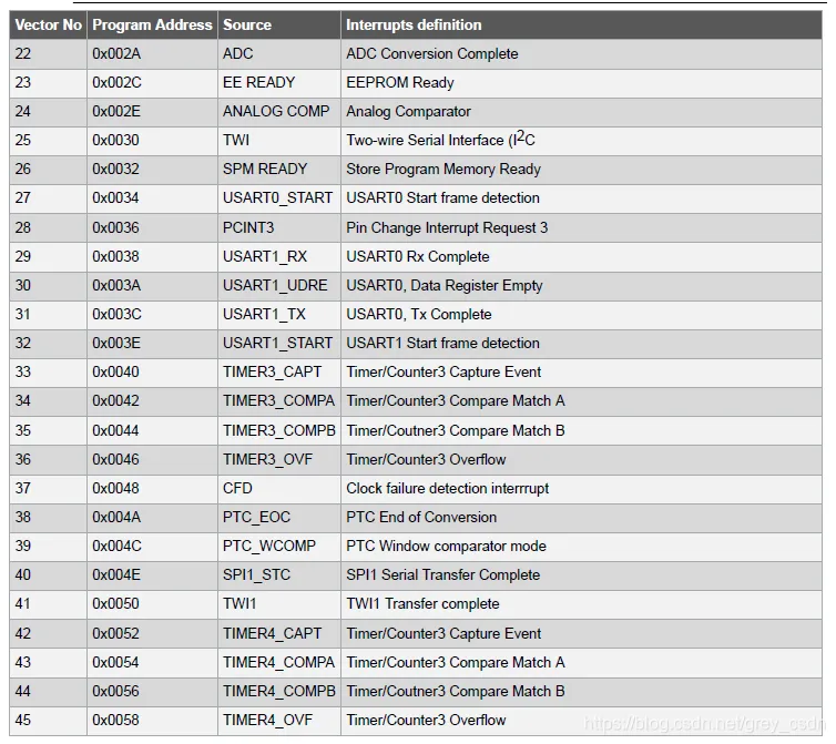
ATmega328P interrupt vector table
6.1.Internal interrupt of ATMega328P
ATMega328P is a single-chip microcomputer from Atmel and belongs to the megaAVR series. The ATMega328P supports a variety of external interrupts, including INT0 and INT112. These interrupts can be triggered by external signals, such as key presses or other sensors.
6.2.External interrupt of ATMega328P
6.3.ATmega328P interrupt handling
(1) When an interrupt occurs,
(2) the microcontroller completes the current instruction,
(3) stores the address of the next instruction on the stack.It also turns off the interrupt system to prevent further interrupts during the interrupt process. This is accomplished by
(4) clearing the SREG global interrupt enable I bit.
(5) The interrupt flag bit is cleared only for type 1 interrupts (see next page for type definition).Execution of the ISR is performed by
(6) loading the program counter with the starting address of the ISR specific to that interrupt. The AVR processor starts running the ISR.
(7) The execution of the ISR continues until the return of the interrupt instruction (reti) is encountered.
(8) SREG I-bit is automatically set (i.e. interrupt is enabled) when executing the reti instruction.
Ⅶ.Serial communication interface of ATMega328P
ATMega328P is a microcontroller from Atmel and belongs to the megaAVR series 12. ATMega328P has a variety of serial communication interfaces, including USART, SPI and I2C.
7.1.USART interface of ATMega328P
The USART is a full-duplex serial communication interface that can be used to communicate with a computer or other device. The USART supports asynchronous and synchronous modes and can be configured through a baud rate generator.
7.2.SPI interface of ATMega328P
SPI is a synchronous serial communication interface that can be used to communicate with other devices, such as memory chips and sensors. SPI uses 4 lines for communication: clock line, data input line, data output line, and chip select line.
7.3.I2C interface of ATMega328P
I2C is a bidirectional serial communication interface that can be used to communicate with other devices, such as temperature sensors and EEPROM chips 34. I2C uses two lines for communication: the serial data line (SDA) and the serial clock line (SCL ).
Ⅷ.Analog input/output port of ATMega328P
8.1.The function of the A/D converter of ATMega328P
The A/D converter of ATMega328P can convert analog signals into digital signals for processing by the microcontroller 12. These converters can be used in many applications such as measuring temperature, light, pressure, humidity, etc.
Datasheets
ATmega328P Automotive - Complete Datasheet
https://ww1.microchip.com/downloads/en/DeviceDoc/Atmel-7810-Automotive-Microcontrollers-ATmega328P_Datasheet.pdf
ATmega48A/PA/88A/PA/168A/PA/328/P Data Sheet
https://ww1.microchip.com/downloads/aemDocuments/documents/MCU08/ProductDocuments/DataSheets/ATmega48A-PA-88A-PA-168A-PA-328-P-DS-DS40002061B.pdf
ATmega48A/PA/88A/PA/168A/PA/328/P Silicon Errata and Data Sheet Clarification
https://ww1.microchip.com/downloads/aemDocuments/documents/MCU08/ProductDocuments/Errata/ATmega48APA88APA168APA328P-SiliConErrataClarif-DS80000855B.pdf
ATmega328P Automotive Silicon Errata and Data Sheet Clarification
https://ww1.microchip.com/downloads/aemDocuments/documents/MCU08/ProductDocuments/Errata/ATmega328P-Auto-SilConErrataClarif-DS80001060.pdf
AN_2585 - AVR151: Setup and use of the SPI on tinyAVR and megaAVR devices
https://ww1.microchip.com/downloads/en/Appnotes/Atmel-2585-Setup-and-Use-of-the-SPI_ApplicationNote_AVR151.pdf
AN_2561 - AVR310: Using the USI Module as a I2C Master
https://ww1.microchip.com/downloads/en/Appnotes/Atmel-2561-Using-the-USI-Module-as-a-I2C-Master_AP-Note_AVR310.pdf
Ⅹ.FAQ
01What are the internal interrupts available in ATMega328P?
ATMega328P has three internal interrupts - INT0, INT1, and PCINT.
02What is the resolution of the A/D converter in Atmega328p?
The A/D converter in Atmega328p has a resolution of 10 bits, which means it can convert an analog input signal into a digital value ranging from 0 to 1023.
03How many analog inputs does Atmega328p have?
The Atmega328p microcontroller has 6 analog inputs that can be used for analog-to-digital conversion. These inputs are labeled as A0 through A5 and are capable of converting analog signals into digital values with a resolution of 10 bits. It is important to note that these pins can also be used as digital input/output pins if needed.
04What is the maximum voltage that can be applied to an analog input pin in Atmega328p?
The maximum voltage that can be applied to an analog input pin in Atmega328p is the same as the operating voltage of the chip, which is typically 5V. However, it is important to note that exceeding this voltage can damage the chip. It is recommended to use a voltage divider or other circuitry to ensure that the voltage applied to the analog input pin is within the safe operating range.
05Are there any limitations or drawbacks to using differential mode in Atmega328p's A/D converter?
Yes, the A/D converter in Atmega328p can be configured to operate in differential mode. This mode allows for the measurement of the voltage difference between two input pins, which can be useful in applications such as sensor signal conditioning.
Related Artilces
ATmega16:Overview,Diagram and Applications
What Arduino Mega 2560 is and How it works


8051 Microcontroller:Features,Applications and Types
Getting Started with Arduino Leonardo Microcontroller
What is ARM7 Based (LPC2148) Microcontroller ?All Explained
ARM Microcontroller : Features,Applications and Function
Embedded Systems vs Microcontrollers: What's the Main Differences?
AC Capacitor Keeps Blowing: What to Do Next?
What is a Fusible Resistor? [Everything You Need to Know]
What is an Air Core Inductor? [Everything Explained]
Unveiling Polypropylene Capacitors: Principles, Applications, and Future Trends
A Primers on Circulator and Isolators


